Research
Research Overview
The Eriksson group pushes the frontier of nanoscale quantum physics in semiconductors. For example, the lab routinely puts Schrodinger’s cat in it’s box — not one made out of cardboard, but semiconductor nanostructures that trap individual electrons (shown left). From here, quantum mechanical phenomena can be explored in these tiny boxes, called quantum dots, to form quantum bits (qubits), the building blocks of quantum computers.
What will you be able to do with a quantum computer? Perform fast search (Grover), efficiently simulate quantum chemistry, and maybe even boost machine learning capabilities — there is a large and growing pool of potential applications. Luckily, it will only take a relatively modest number of qubits to achieve important new capabilities, because of a phenomenon known as quantum “parallelism.”
The Eriksson lab studies (and builds small quantum computers!) with qubits that are dense, fast, and industry compatible. This is because the technology parallels the existing infrastructure of the classical bit, which has the ability to pack billions of transistors into tiny computer chips. One of our primary goals is to demonstrate scalable quantum information processing using industry-mature semiconductor technology.
A good quantum computer fulfills the DiVincenzo requirements. These include two-qubit quantum gates, single-qubit coherence and control, qubit-photon coupling, and scalability, as outlined below. The underlying physics behind these qubits is also explored through novel fabrication methods, quantum dot spectroscopy, and Hall Bar measurements. Furthermore, thermal transport in thin two-dimensional materials is investigated for applications in thermal management in nanoelectronics.
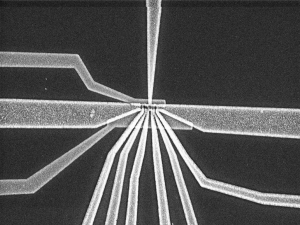
Members of the Eriksson lab use a wide range of skills and resources to conduct this research. Devices are typically fabricated using a combination of photolithography and electron-beam lithography in the University’s cleanroom to pattern nanostructures such as the ones shown above. Measurements are performed at temperatures as cold as 15 mK in dilution refrigerators with magnetic fields as high as 14 T. Ultra-low noise measurements and precision electronics are used in qubit experiments, which we manipulate on time scales as short as 20 ps.
High-fidelity two-qubit gates are a key ingredient for quantum computation. Generating these gates requires the electrons to interact with each other in a finely controlled way. For individual electron spins in silicon, this is mediated by the Heisenberg exchange interaction, and opens the doors to a universal gate set which can perform two-qubit quantum computations such as the Deutsch-Josza and Grover algorithms [1]. Two-qubit gate fidelities are improving, now above 90% [2], and is approaching the fault-tolerant threshold.
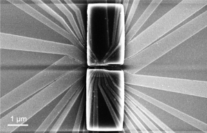
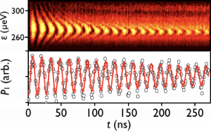
Alternative encodings such as the quantum dot hybrid qubit (QDHQ) allow for faster two-qubit gate speeds due to its strong dipole coupling and fidelities above fault tolerance may be feasible by utilizing the QDHQ’s dynamical sweet spots [3]. Quadruple quantum dot devices in silicon show large dipole couplings [4] and conditional rotations demonstrated on two double-dot qubits in the charge-like regime show impressive performance speeds (74 ps) [5].
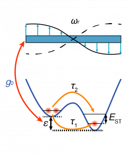
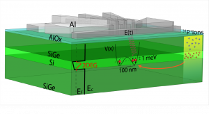
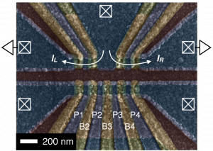
Interconverting stationary to flying qubits is necessary for scaling quantum-dot qubits and building a quantum network. We utilize resonators made of Nb, NbN, or TiN to strongly couple the quantum dot’s energy levels to the photonic mode in the resonator. Sufficient coupling strength and coherence times allows for dispersive readout of the quantum dot charge state and photon-mediated two-qubit gates across well-separated qubits.
This approach imposes stringent conditions on the qubit — it must display strong dipolar coupling yet robust coherence properties. Due to its simultaneous charge and spin nature, the QDHQ provides an exciting platform for coupling to a microwave cavity. In the charge regime, the qubit displays strong dipolar coupling, while the best coherence properties are found in the far-detuned regime. The QDHQ can be tuned to sweet spots which exhibit both properties allowing the optimization of well-separated two-qubit gates.
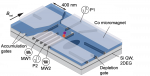
Every flavor of qubit offers tradeoffs in speed, coherence, fabrication resources, control requirements, and cooling budget. Loss-Divincenzo spin qubits in silicon require dc magnetic fields but are relatively insensitive to charge noise. Integrating micromagnets on the silicon device considerably speeds up gate operations in such qubits [6].
The quantum dot hybrid qubit (QDHQ) is a particular flavor native to Wisconsin [7]. It offers an improvement in gate time, a charge-noise protective sweet spot, and removes any need for magnetic control. The QDHQ was first realized in a doped depletion-mode Si/SiGe device [8], and variants of this qubit are explored with overlapping accumulation-mode devices in undoped Si/SiGe [9].
The qubit’s energy structure relies on the singlet-triplet splitting, which is related to the valley physics and Coulomb interaction in the multi-electron dot. This parameter can be tuned by controlling the surrounding electrostatic environment of the quantum dot. Methods to optimally readout and manipulate this qubit are continually explored in the lab, and gate fidelities above 99.9% may be achievable in the strong-driving regime [11].
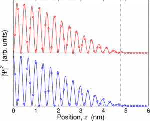
Silicon has a six-fold degeneracy in the conduction band that is lifted by strain in the Si/SiGe heterostructure. The two lowest remaining states are separated in energy by the valley splitting, which is sensitive to the details of the interface profile in the quantum well. Understanding and controlling the valley splitting is important for qubit platforms in silicon. Two-qubit gates with single spins and single-qubit gates with multi-electron qubits (such as the QDHQ) rely on the singlet-triplet (ST) splitting, which depends on the valley physics in the quantum dot.
Previously, the singlet-triplet splitting was adjusted by translating the dot across the quantum well interface [13]. Furthermore, novel Si/SiGe heterostructures may offer improved electrical control of the singlet-triplet splitting. The Eriksson group collaborates with the Friesen, Joynt, and Lagally groups to engineer and grow custom silicon-germanium layer stacks with the Lagally-group chemical vapor deposition (CVD) tool.
Auto-tuning
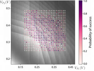
Eriksson members at present usually “tune-up” all of their quantum devices by hand — tweaking voltages on a handful of gates to form quantum dots. Eventually, computers will have to take over when the device complexity increases. Collaborators at NIST have developed machine learning algorithms to identify the key features of quantum dots and appropriately adjusted voltages to achieve the single electron regime [14].
Flip-chip technology
Scalable quantum-to-classical electronic interconnects is a paramount ingredient in a large quantum computer. Most chips are wire-bonded to printed circuit boards at ~ 20 mK. However, this technique will soon be infeasible as devices become larger. An alternative approach is to use flip-chip technology that provides dense bump bonds for electrical connection between the quantum chips and the classical circuit board. Flip-chip bonding also offers improved RF performance and reduced parasitic capacitance to each signal line. These features are especially advantageous with resonator-dot devices that require cavities with high quality factors. Additionally, flip chipping allows the resonator to be patterned on a separate substrate, avoiding some of the contracting fabrication requirements between high-Q resonators and quantum dots (such as the need for dielectrics). We collaborate with William D. Oliver and the superconducting qubit team at the MIT campus & Lincoln Laboratory on flip-chip resonators coupled to our quantum dot devices.
Multiplexing
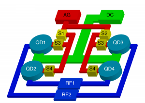
The CPU processor in a computer has on order a million transistors for every input-output connection. The silicon industry achieves this through multiplexing techniques, packing billions of transistors inside a small computer chip. Quantum dot devices currently require order 10-20 electrical connections for only a few qubits. Similar techniques will need to be utilized to push semiconductor quantum processors to the 1000+ qubit regime.
For example, on-chip field effect transistors can switch between different current paths in a quantum dot array, greatly reducing the number of input-output connections for every dot [15]. This technique can be used to fabricate large arrays of spatially separated quantum dots which can probe how device characteristics (such as valley splitting or charge noise) vary across a Si/SiGe wafer.
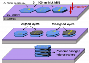
Thermal conductivity is measured using the three-omega method on a wide variety thin film structures to investigate how phonons, the primary heat carriers in non-metals at room temperature, propagate across material interfaces. Past work has focused on III-V ternary alloy superlattices which contain high densities of material interfaces [16]. Currently, thermal transport across films of two-dimensional materials such as hexagonal boron nitride (hBN) and graphite (Gr) is studied. These films are so thin that many of the phonons travel ballistically across the entire film without scattering. In this quasi-ballistic transport regime, the thermal properties of materials diverge strongly from that of large bulk crystals. Understanding thermal transport at these short length-scales is critical for thermal management applications in nanoelectronics devices.
Referenced Citations
[1] “A programmable two-qubit quantum processor in silicon.” T. F. Watson, S. G. J. Philips, E. Kawakami, D. R. Ward, P. Scarlino, M. Veldhorst, D. E. Savage, M. G. Lagally, Mark Friesen, S. N. Coppersmith, M. A. Eriksson, and L. M. K. Vandersypen, Nature 555, 633 (2018) [2] “Benchmarking Gate Fidelities in a Si/SiGe Two-Qubit Device.” X. Xue, T. F. Watson, J. Helsen, D. R. Ward, D. E. Savage, M. G. Lagally, S. N. Coppersmith, M. A. Eriksson, S. Wehner, and L. M. K. Vandersypen, Phys. Rev. X 9, 021011 (2019) [3] “Adiabatic two-qubit gates in capacitively coupled quantum dot hybrid qubits,” Adam Frees, Sebastian Mehl, John King Gamble, Mark Friesen, and S. N. Coppersmith, npj Quantum Inform. 5, 73 (2019) [4] “Measurements of capacitive coupling within a quadruple quantum dot array.” S. F. Neyens, E. R. MacQuarrie, J. P. Dodson, J. Corrigan, Nathan Holman, B. Thorgrimsson, M. Palma, T. McJunkin, L. F. Edge, Mark Friesen, S. N. Coppersmith, and M. A. Eriksson, Phys. Rev. Applied 12, 064049 (2019) [5] “Progress Towards a Capacitively Mediated CNOT Between Two Charge Qubits in Si/SiGe.” E. R. MacQuarrie, S. F. Neyens, J. P. Dodson, J. Corrigan, B. Thorgrimsson, Nathan Holman, M. Palma, L. F. Edge, Mark Friesen, S. N. Coppersmith, and M. A. Eriksson, arXiv:2003.06768 (2020) [6] “Electrical control of a long-lived spin qubit in a Si/SiGe quantum dot.” E. Kawakami, P. Scarlino, D. R. Ward, F. R. Braakman, D. E. Savage, M. G. Lagally, Mark Friesen, S. N. Coppersmith, M. A. Eriksson, and L. M. K. Vandersypen, Nature Nanotech. 9, 666 (2014) [7] “Fast Hybrid Silicon Double-Quantum-Dot Qubit.” Zhan Shi, C. B. Simmons, J. R. Prance, John King Gamble, Teck Seng Koh, Yun-Pil Shim, Xuedong Hu, D. E. Savage, M. G. Lagally, M. A. Eriksson, Mark Friesen, and S. N. Coppersmith, Phys. Rev. Lett. 108, 140503 (2012) [8] “Quantum control and process tomography of a semiconductor quantum dot hybrid qubit.” Dohun Kim, Zhan Shi, C. B. Simmons, D. R. Ward, J. R. Prance, Teck Seng Koh, John King Gamble, D. E. Savage, M. G. Lagally, Mark Friesen, S. N. Coppersmith, and M. A. Eriksson, Nature 511, 70 (2014) [10] “Extending the coherence of a quantum dot hybrid qubit.” B. Thorgrimsson, Dohun Kim, Yuan-Chi Yang, L. W. Smith, C. B. Simmons, D. R. Ward, R. H. Foote, J. Corrigan, D. E. Savage, M. G. Lagally, Mark Friesen, S. N. Coppersmith, and M. A. Eriksson, npj Quant. Inf. 3, 32 (2017) [11] “High-fidelity single-qubit gates in a strongly driven quantum-dot hybrid qubit with 1/f charge noise,” Yuan-Chi Yang, S. N. Coppersmith, and Mark Friesen, Phys. Rev. A 100, 022337 (2019) [12] “Valley splitting theory of SiGe∕Si∕SiGe quantum wells,” Mark Friesen, Sucismita Chutia, Charles Tahan, and S. N. Coppersmith Phys. Rev. B 75, 115318 (2007) [13] “Tunable singlet-triplet splitting in a few-electron Si/SiGe quantum dot.” Zhan Shi, C. B. Simmons, J. R. Prance, John King Gamble, Mark Friesen, D. E. Savage, M. G. Lagally, S. N. Coppersmith, and M. A. Eriksson, Appl. Phys. Lett. 99, 233108 (2011) [14] “Auto-tuning of double dot devices in situ with machine learning.” Justyna P. Zwolak, T. McJunkin, Sandesh S. Kalantre, J. P. Dodson, E. R. MacQuarrie, D. E. Savage, M. G. Lagally, S. N. Coppersmith, M. A. Eriksson, and Jacob M. Taylor, Phys. Rev. Applied 13, 034075 (2020) [15] “Integration of on-chip field-effect transistor switches with dopantless Si/SiGe quantum dots for high-throughput testing.” D. R. Ward, D. E. Savage, M. G. Lagally, S. N. Coppersmith, and M. A. Eriksson, Appl. Phys. Lett. 102, 213107 (2013) [16] “Measurements of the Thermal Resistivity of InAlAs, InGaAs, and InAlAs/InGaAs Superlattices.” G. R. Jaffe, S. Mei, C. Boyle, J. D. Kirch, D. E. Savage, D. Botez, L. J. Mawst, I. Knezevic, M. G. Lagally, and M. A. Eriksson, ACS Appl. Mat. Int. 11, 11970 (2019)